Plan Optik is the leading manufacturer of customized glass wafers! With it’s new “Advanced Conncectivity Technology (ACT)” Plan Optik developed a solution to create or refine products for advanced packaging, 6G or other connectivity and high frequency applications.
Design Rules
The following are used to get a initial overview. The entire range of services is not limited to these specifications. For more information and to discuss your individual project, please contact us at contact@planoptik.com.
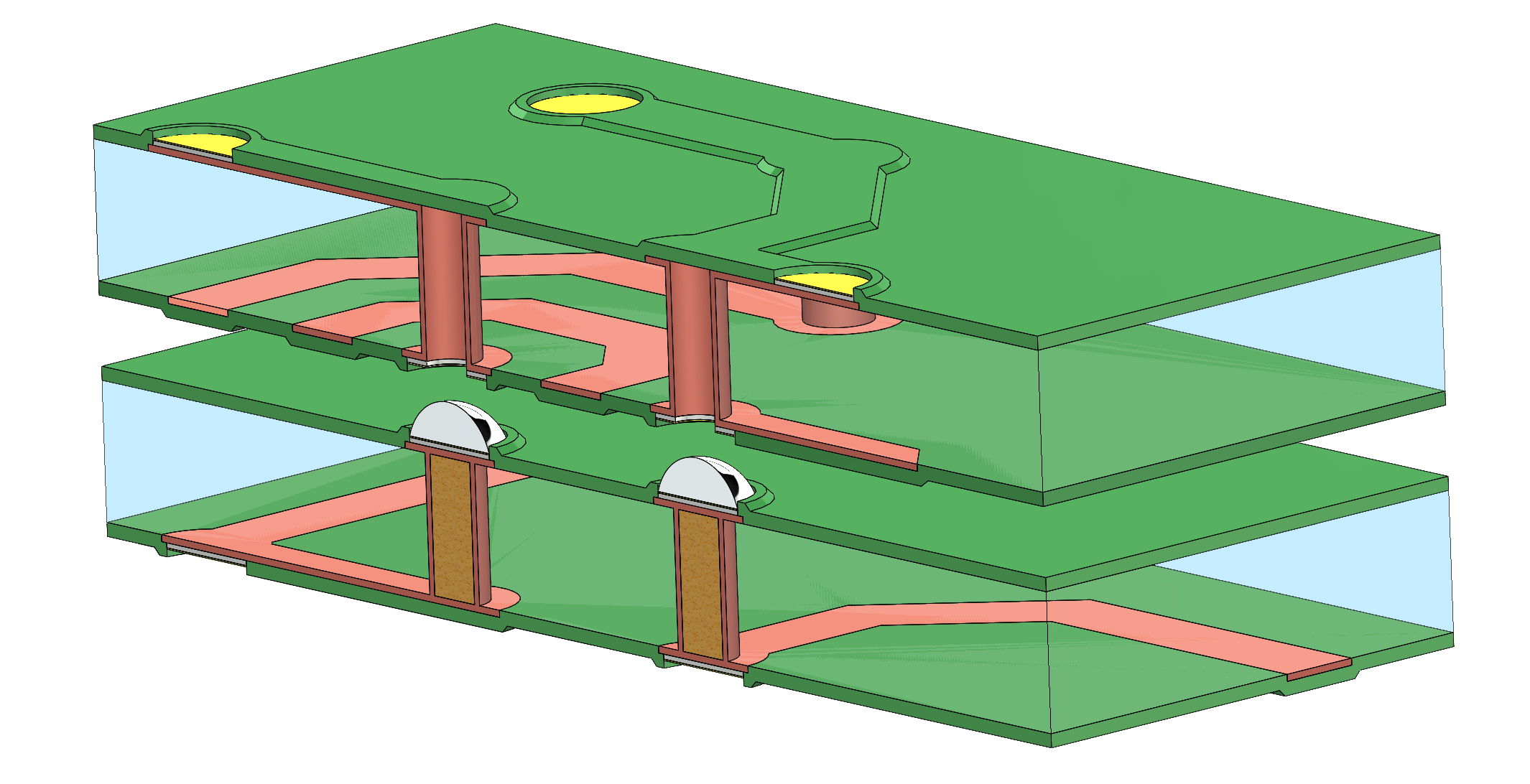
Through Glass Vias - Characteristics
Description | Available | Under Development |
Material | Borofloat33 | Others |
Wafer Diameter | up to 300mm | |
Panel Dimension | up to 200 x 200 mm | |
Substrate thickness | 300 – 1000 µm | 150 – 1500 µm |
Hole diameter | ≥100 µm | <100 µm |
Pitch | twice hole diameter | smaller |
Customized RDL | Up to 200mm diameter | |
Cu thickness | 3..10 µm | 2..15 µm |
Line / Space | 50µm/50µm |
Applications
Products and Services

INTERPOSER ACT

GLASS-CIRCUIT-BOARDS ACT

METALLIZATION ACT

REDISTRIBUTION LAYER ACT
Above you can find some products and services which can or could be achieved with ACT. The target possibilities which are being planned and and the things we are actually working on can be viewed in the “next steps” area. Initial specifications, which are used to get a first overview, can be found in the section “Design Rules”. For more information please do not hesitate to contact us at sales@planoptik.com.